8
error amplifier (Error Amp) output (V
E/A
) is compared with
the oscillator (OSC) triangular wave to provide a pulse-width
modulated (PWM) wave with an amplitude of V
IN
at the
PHASE node. The PWM wave is smoothed by the output
filter (L
O
and C
O
).
The modulator transfer function is the small-signal transfer
function of V
OUT
/V
E/A
. This function is dominated by a DC
Gain, given by V
IN
/V
OSC
, and shaped by the output filter, with
a double pole break frequency at F
LC
and a zero at F
ESR
.
Modulator Break Frequency Equations
The compensation network consists of the error amplifier
(internal to the ISL6432) and the impedance networks Z
IN
and Z
FB
. The goal of the compensation network is to provide
a closed loop transfer function with high 0dB crossing
frequency (f
0dB
) and adequate phase margin. Phase margin
is the difference between the closed loop phase at f
0dB
and
180 degrees. The equations below relate the compensation
networks poles, zeros and gain to the components (R1, R2,
R3, C1, C2, and C3) in Figure 6. Use these guidelines for
locating the poles and zeros of the compensation network:
1. Pick Gain (R2/R1) for desired converter bandwidth
2. Place 1
ST
Zero Below Filters Double Pole (~75% F
LC
)
3. Place 2
ND
Zero at Filters Double Pole
4. Place 1
ST
Pole at the ESR Zero
5. Place 2
ND
Pole at Half the Switching Frequency
6. Check Gain against Error Amplifiers Open-Loop Gain
7. Estimate Phase Margin - Repeat if Necessary
Compensation Break Frequency Equations
Figure 6 shows an asymptotic plot of the DC-DC converters
gain vs. frequency. The actual Modulator Gain has a high gain
peak dependent on the quality factor (Q) of the output filter,
which is not shown in Figure 6. Using the above guidelines
should yield a Compensation Gain similar to the curve plotted.
The open loop error amplifier gain bounds the compensation
gain. Check the compensation gain at F
P2
with the capabilities
of the error amplifier. The Closed Loop Gain is constructed on
the log-log graph of Figure 10 by adding the Modulator Gain (in
dB) to the Compensation Gain (in dB). This is equivalent to
multiplying the modulator transfer function to the compensation
transfer function and plotting the gain.
The compensation gain uses external impedance networks
Z
FB
and Z
IN
to provide a stable, high bandwidth (BW) overall
loop. A stable control loop has a gain crossing with
-20dB/decade slope and a phase margin greater than 45
degrees. Include worst case component variations when
determining phase margin.
ACPI Implementation
The three linear controllers included within the ISL6432 can
independently be shut down, in order to accommodate
Advanced Configuration and Power Interface (ACPI) power
management features.
To shut down any of the linears, one needs to pull and keep
high the respective FB pin above a typical threshold of 1.25V.
One way to achieve this task is by using a logic gate coupled
through a small-signal diode. The diode should be placed as
close to the FB pin as possible to minimize stray capacitance
to this pin. Upon turn-off of the pull-up device, the respective
output undergoes a soft-start cycle, bringing the output within
regulation limits. On the regulators implementing this feature,
the parallel combination of the feedback resistors has to be
sufficiently high to allow ease of driving from the external
device. Considering the other restriction applying to the upper
range of this resistor combination (see Output Voltage
Selection paragraph), it is recommended the values of the
feedback resistors on an ACPI-enabled linear regulator output
meet the following constraint:
To turn off the switching regulator, use an open-drain or
open-collector device capable of pulling the OCSET pin (with
the attached R
OCSET
pull-up) below 1.25V. To minimize the
possibility of OC trips at levels different than predicted, a
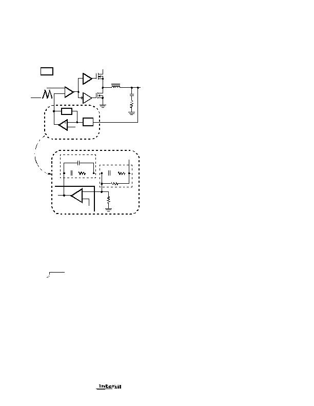
FIGURE 5. VOLTAGE-MODE BUCK CONVERTER
COMPENSATION DESIGN
V
OUT
OSC
0.8V
L
O
C
O
ESR
V
IN
V
OSC
ERROR
AMP
PWM
DRIVER1
(PARASITIC)
Z
FB
+
-
0.8V
R
S1
R3
R2
C3
C2
C1
COMP
V
OUT
FB
Z
FB
ISL6432
Z
IN
COMP
DRIVER
DETAILED COMPENSATION COMPONENTS
PHASE
V
E/A
+
-
Z
IN
R
P1
SYNC
+
+
F
LC
1
2?/DIV>
L
O
C
O
?/DIV>
?/DIV>
--------------------------------------- -
=
F
ESR
1
2?nbsp ESR C
O
?/DIV>
?/DIV>
---------------------------------------- -
=
F
Z1
1
2?nbsp R
?nbsp 2 C1
?/DIV>
-----------------------------------
=
F
Z2
1
2?nbsp R
S1
R3
+
(
) C3
?/DIV>
?/DIV>
--------------------------------------------------------- -
=
F
P1
1
2?nbsp R
2
C1 C2
?/DIV>
C1 C2
+
--------------------- -
?/DIV>
?/DIV>
?/DIV>
?/DIV>
?/DIV>
?/DIV>
------------------------------------------------------ -
=
F
P2
1
2?nbsp R
?nbsp 3 C3
?/DIV>
-----------------------------------
=
2k&
R
S
R
P
?/DIV>
R
S
R
P
+
--------------------- - 5k&
<
<
ISL6432
发布紧急采购,3分钟左右您将得到回复。
相关PDF资料
ISL6521CBZS2698
IC REG QD BCK/LINEAR 16-SOIC
ISL6528CBZ-TS2698
IC REG DL BCK/LINEAR SYNC 8-SOIC
ISL6529CBZ
IC REG DL BCK/LINEAR SYNC 14SOIC
ISL6534CVZ-TR5229
IC REG 3OUT BCK/LINEAR 24EPTSSOP
ISL6549CRZR5213
IC REG DL BCK/LINEAR SYNC 16-QFN
ISL9305IRTHWLNCZ-T
IC REG QD BUCK/LINEAR 16TQFN
ISL9305IRTWLNCZ-T
IC REG QD BUCK/LINEAR 16TQFN
ISL9307IRTWCWNZ-T
IC REG QD BCK/LINEAR SYNC 16TQFN
相关代理商/技术参数
ISL6433BCB
制造商:Intersil Corporation 功能描述:
ISL6434CB
制造商:Intersil Corporation 功能描述:
ISL6435CA
制造商:Intersil Corporation 功能描述:
ISL6436HIB
制造商:Intersil Corporation 功能描述:
ISL6436LIB
功能描述:IC CTRLR PS USB DUAL PORT 8-SOIC RoHS:否 类别:集成电路 (IC) >> 接口 - 控制器 系列:- 标准包装:4,900 系列:- 控制器类型:USB 2.0 控制器 接口:串行 电源电压:3 V ~ 3.6 V 电流 - 电源:135mA 工作温度:0°C ~ 70°C 安装类型:表面贴装 封装/外壳:36-VFQFN 裸露焊盘 供应商设备封装:36-QFN(6x6) 包装:* 其它名称:Q6396337A
ISL6439ACB
制造商:Rochester Electronics LLC 功能描述:- Bulk 制造商:Intersil Corporation 功能描述:
ISL6439ACB-T
制造商:Rochester Electronics LLC 功能描述:- Bulk 制造商:Intersil Corporation 功能描述:
ISL6439ACR
制造商:Rochester Electronics LLC 功能描述:- Bulk 制造商:Intersil Corporation 功能描述: